Synopsis: Exploring top Indian States which offer land for the semiconductor industry, subsidies, Government initiatives and policy, and recent projects.
The fastest growing economy, India, is focusing more on the semiconductor industry. Now, India is not only a leader in the service sector, but it is also fast emerging as a global manufacturing hub. Based on the latest policies and announcements as of 2025, five states stand out for their robust land related benefits and infrastructure commitments.
1. Uttar Pradesh

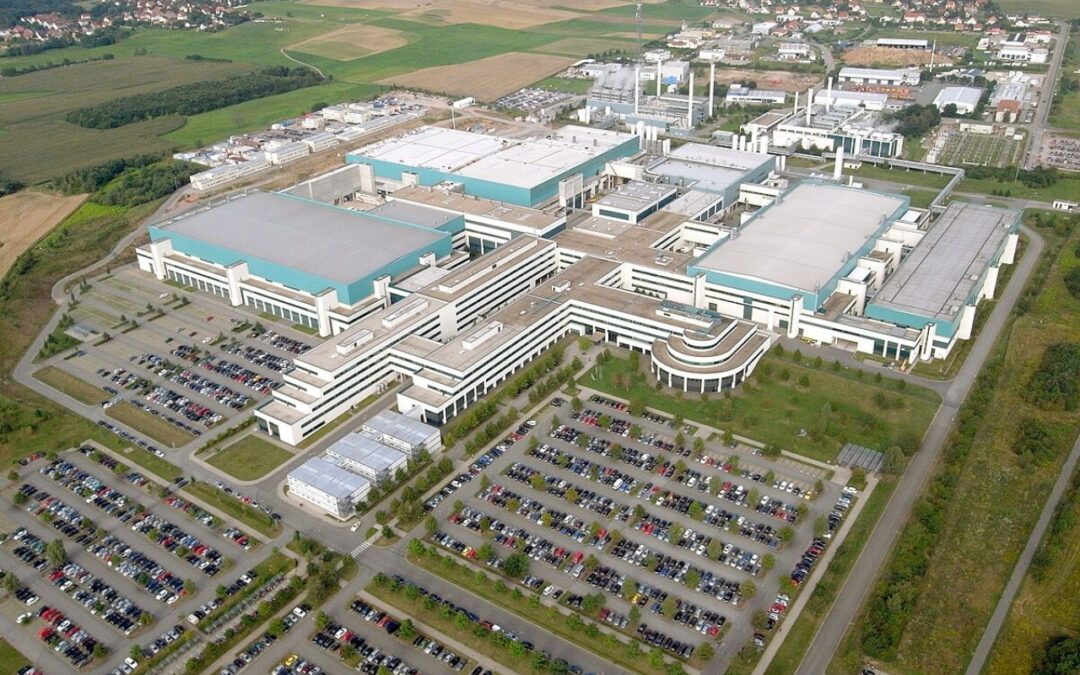
Uttar Pradesh has positioned itself as a front-runner with its Semiconductor policy 2024, offering among the most aggressive land subsidies in the country. The state accounts for 45% of India’s smartphone manufacturing and 55% of mobile components. UP has an important centre for exporting consumer electronics which are global brands like Samsung, Oppo, Vivi, Dixon technologies, Sunwoda, Haier.
Samsung has opened its largest mobile manufacturing plant in Noida. And UP partners with HCL Group and Foxconn are jointly developing the plant at Jewar, UP. The production is expected to begin in 2027.
Land and Financial Incentives
UP government has dedicated over 1,000 acres as a semiconductor-specific park with ready-made Infrastructure, providing a turnkey solution for manufacturers:
- 75% subsidy on the first 200 acres from state land agencies, 30% subsidy on additional land.
- 100% exemption on stamp duty and land registration fees.
- 5% per annum interest subsidy for 7 Years.
- 100% state GST reimbursement for 6-16 years.
2. Gujarat

Gujarat became India’s first state to implement a dedicated semiconductor policy and already hosts a functioning semiconductor facility in Dholera. Dholera encompasses 920 square kilometers as a planned greenfield industrial city.
Approved Projects and Capacity
| Project | Investment | Capacity | Status |
| Tata Electronic Fab (Dholera) | ₹91,000 crore | 50,000 wafers/ month | Under construction; targeting late-2026 for first chips |
| Micron ATMP (Sanand) | $2.75 billion | Advanced Packaging/testWhich create 15,000 jobs | 60% construction complete; operational /near operational by H1 2025. |
Land & Financial Incentives
Gujarat is providing similar incentives like UP, Dholera is being developed as “Semicon city”
- 75% subsidy on the first 200 acres in Dholera
- 100% one time refund on stamp duty and registration fees
- 40% additional subsidy on central government capital expenditure support.
- ₹2 per unit electricity subsidy for 10 years.
3. Odisha
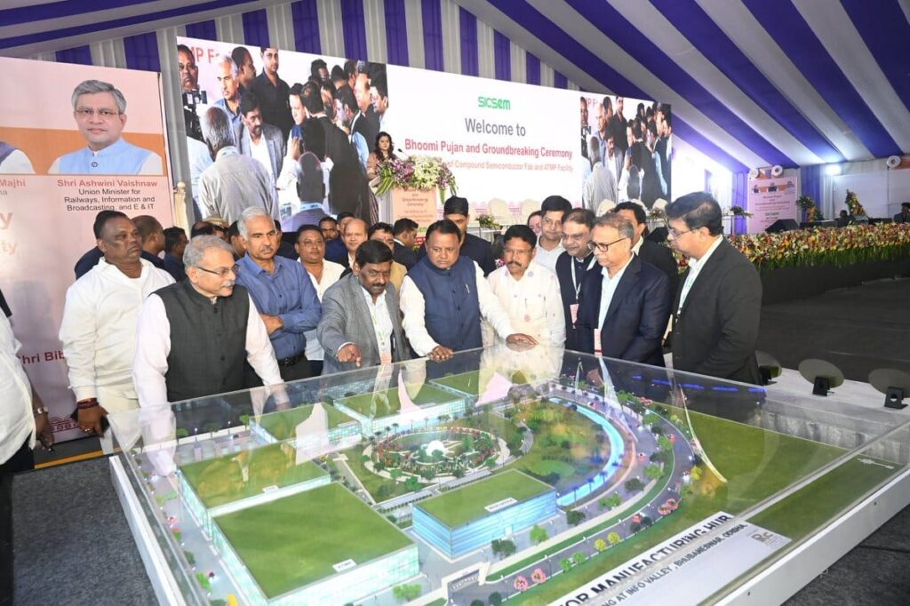
Odisha capital city Bhubaneswar has been designated as a semiconductor hub with projects concentrated in Info Valley near IIT Bhu. The semiconductor and ESDM (Electronic System Design and manufacturing) park will span 200 acres directly adjacent to IIT Bhubaneswar campus.
Approved Projects & Technology Focus
| Project | Company | Investment | Capacity | Technology |
| SiC Fab – India’s First Commercial | SiCSem Pvt Ltd and UK’s Clas-Sic | ₹2,067 Cr | 60,000 Wafters/year with 96 million packaged units | Silicon Carbide for Defense, EVs, rail, data centers |
| 3D Glass Integration | 3D Glass Solution Inc | ₹2,044 Cr | 69,600 glass panel substrates/year + 50M assembled units +13,200 3DHI modules | 3D heterogeneous integration for AI,RF, photonics, co-packaged optics. |
SiC semiconductors are crucial for EVs, renewable energy and high power application. That offers higher efficiency with lower switching, increased power density with 3-5 X faster switching speeds, reduced vehicle weight and size and extended EV driving range.
Land & Financial Incentives
- 25% discount over IPR rates for the first 5 projects means the Investment > ₹5000 cr.
- 10% subsidy for subsequent mega projects on the first 200 acres.
- 100% exemption on stamp duty for lease/ sale agreement.
- ₹2 per unit power tariff reimbursement for 10years
- 5% per annum interest subsidy for 7 Years (₹50 cr cap).
Also read: 7 Emerging Industrial Hubs Driving India’s Semiconductor Growth with Strong Investment Opportunities
4. Assam
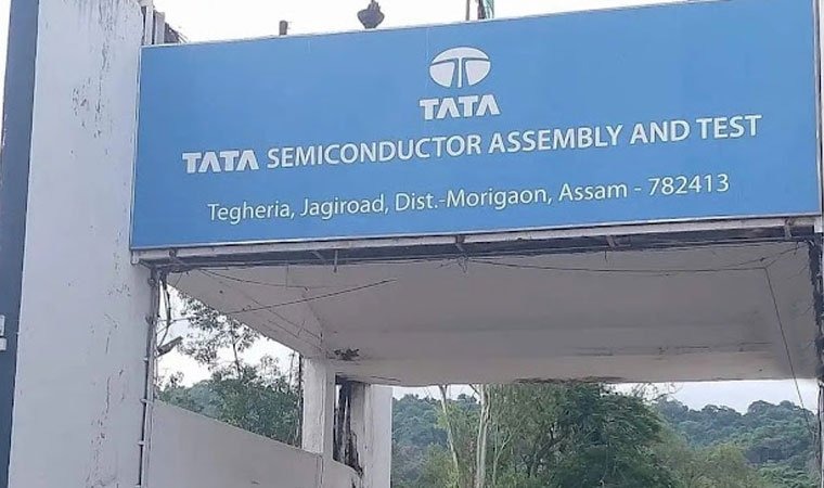
Assam has a strategic location in Jagiroad, Morigaon district, approximately 150km from Guwahati on the site of a former Hindustan Paper Corporation’s Nagaon paper Mill where the Tata Semiconductor Assembly & Test facility is located.
Approved Project & Employment
| Project | Company | Investment | Capacity |
| Tata ATMP | Tata Semiconductor Assembly & Test(TSAT) | ₹27,000 Cr | 48 Million chips/days, 60,000 wafers/year equivalent |
The ATMP facility is focused on Assembly,Testing, Marking, and packaging. The product targets EVs, communication and Network infrastructure, Defense and aerospace applications.
Land & Financial Incentives:
- 100% exemption on stamp duty for lease/ sale agreements
- 40% additional capital expenditure assistance
- 50% power tariff subsidy for 10 years
- ₹5 per cubic meter water supply for first 10 year
- 100% SGST reimbursement
5. Andhra Pradesh
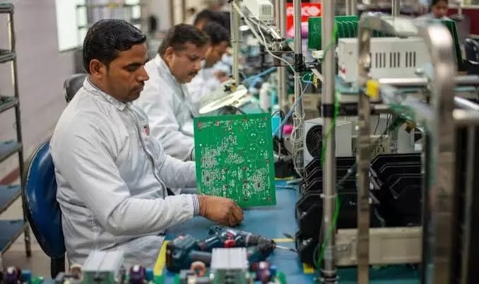
AP has established itself as a leading exporter gateway for electronics manufacturers in India, with a strategic focus on Electronic Manufacturing Clusters (EMCs) and component production.
- Tripathi Electronic Manufacturing Cluster has attracted Dixon Technologies and TCL Electronics.
- Orvakal Mega Industrial Park which is in Kurnool District, for Silicon Carbide (SiC) specialty semiconductor manufacturing for advanced applications.
Approved Projects & Capacity
| Project | Company | Location | Investment | Applications |
| Advanced Packaging Unit | ASIP (with South Korea’s APACT) | Tirupati EMC | ₹468 Cr | Mobile phones, set-top boxes, automotive, household electronic |
| Silicon Carbide Fab | Indichip + Japan’s YITOA Micro | Orvakal, Kurnool | ₹14,000 Cr | EVs, renewable energy, high-power applications |
Andhra Pradesh has Dual Location strategy, 5000 acres within 2 hours of Chennai airport (electronic supplier base). Another is 5,000 acres within 2 hours of Bangalore airport(IT hub).
Land & Financial Incentives:
- 10,000 acres earmarked with infrastructure-ready zones
- 50% additional financial incentives to projects approved under central schemes
- Electricity duty exemptions for 10 years
- Power tariff reimbursements
- Assured water supply at project sites
- Land cost incentives and stamp duty concessions
Conclusion
India is transitioning from a strong position in semiconductor design to becoming a more significant player in manufacturing, leveraging government support by providing subsidy, exempted in stamp duty, GST cut and more. There are a lot of upcoming projects also there. By 2030 India will become a $100-110 billion semiconductor market.
Written by Yatheendra N